- 您现在的位置:买卖IC网 > Sheet目录1213 > EVAL-AD7741/42EBZ (Analog Devices Inc)BOARD EVAL FOR AD7741/7742
�� �
�
�AD7741/AD7742�
�Isolation� Applications�
�In� addition� to� analog-to-digital� conversion,� the� AD7741/AD7742�
�can� be� used� in� isolated� analog� signal� transmission� applications.�
�Due� to� noise,� safety� requirements� or� distance,� it� may� be� neces-�
�sary� to� isolate� the� AD7741/AD7742� from� any� controlling�
�circuitry.� This� can� easily� be� achieved� by� using� opto-isolators,�
�which� will� provide� isolation� in� excess� of� 3� kV.�
�Opto-electronic� coupling� is� a� popular� method� of� isolated� signal�
�coupling.� In� this� type� of� device,� the� signal� is� coupled� from� an�
�input� LED� to� an� output� photo-transistor,� with� light� as� the� con-�
�necting� medium.� This� technique� allows� dc� to� be� transmitted,� is�
�extremely� useful� in� overcoming� ground� loops� between� equip-�
�ment,� and� is� applicable� over� a� wide� range� of� speeds� and� power.�
�The� analog� voltage� to� be� transmitted� is� converted� to� a� pulse�
�train� using� the� VFC.� An� opto-isolator� circuit� is� used� to� couple�
�this� pulse� train� across� an� isolation� barrier� using� light� as� the�
�connecting� medium.� The� input� LED� of� the� isolator� is� driven�
�from� the� output� of� the� AD7741/AD7742.� At� the� receiver� side,�
�the� output� transistor� is� operated� in� the� photo-transistor� mode.�
�The� pulse� train� can� be� reconverted� to� an� analog� voltage� using� a�
�frequency-to-voltage� converter;� alternatively,� the� pulse� train� can�
�be� fed� into� a� counter� to� generate� a� digital� signal.�
�The� analog� and� digital� sections� of� the� AD7741/AD7742� have�
�been� designed� to� allow� operation� from� a� single-ended� power�
�source,� simplifying� its� use� with� isolated� power� supplies.�
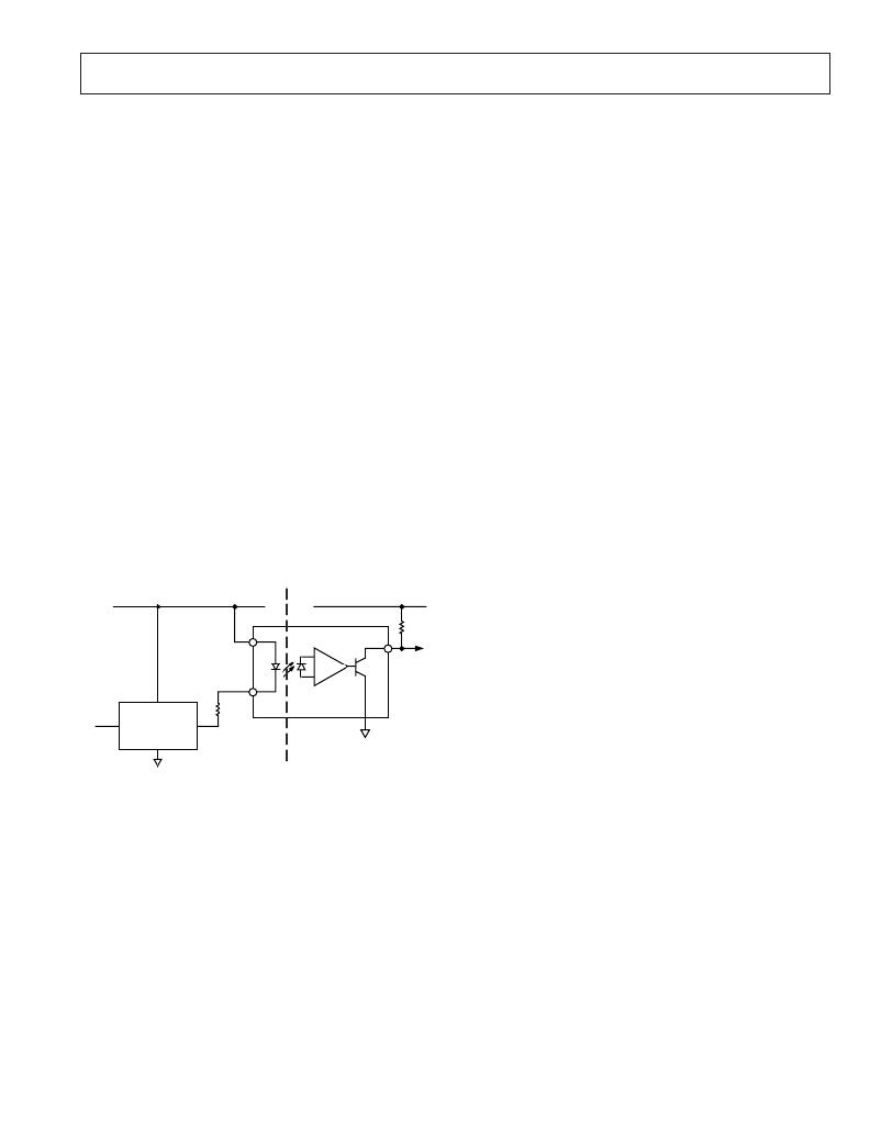
�Figure� 12� shows� a� general� purpose� VFC� circuit� using� a� low� cost�
�opto-isolator.� A� +5� V� power� supply� is� assumed� for� both� the�
�isolated� (+5� V� isolated)� and� local� (+5� V� local)� supplies.�
�Power� Supply� Bypassing� and� Grounding�
�In� any� circuit� where� accuracy� is� important,� careful� consideration�
�of� the� power� supply� and� ground� return� layout� helps� to� ensure�
�the� rated� performance.� The� printed� circuit� board� housing� the�
�AD7741/AD7742� should� be� designed� so� the� analog� and� digital�
�sections� are� separated� and� confined� to� certain� areas� of� the� board.�
�To� minimize� capacitive� coupling� between� them,� digital� and�
�analog� ground� planes� should� only� be� joined� in� one� place,� close�
�to� the� DUT� and� should� not� overlap.�
�Avoid� running� digital� lines� under� the� device� as� these� will� couple�
�noise� onto� the� die.� The� analog� ground� plane� should� be� allowed�
�to� run� under� the� AD7742� to� avoid� noise� coupling.� The� power�
�supply� lines� to� the� AD7742� should� use� as� large� a� trace� as� pos-�
�sible� to� provide� low� impedance� paths� and� reduce� the� effects� of�
�glitches� on� the� power� supply� line.� Fast� switching� signals� like�
�clocks� should� be� shielded� with� digital� ground� to� avoid� radiating�
�noise� to� other� parts� of� the� board� and� clock� signals� should� never�
�be� run� near� analog� inputs.� Avoid� crossover� of� digital� and� analog�
�signals.� Traces� on� opposite� sides� of� the� board� should� run� at�
�right� angles� to� each� other.� This� reduces� the� effect� of� feedthrough�
�through� the� board.� A� microstrip� technique� is� by� far� the� best� but�
�is� not� always� possible� with� a� double-sided� board.� In� this� tech-�
�nique,� the� component� side� of� the� board� is� dedicated� to� the� ground�
�plane� while� the� signal� traces� are� placed� on� the� solder� side.�
�Good� decoupling� is� also� important.� All� analog� supplies� should�
�be� decoupled� to� GND� with� surface� mount� capacitors,� 10� μ� F� in�
�parallel� with� 0.1� μ� F� located� as� close� to� the� package� as� possible,�
�ideally� right� up� against� the� device.� The� lead� lengths� on� the� by-�
�pass� capacitor� should� be� as� short� as� possible.� It� is� essential� that�
�these� capacitors� be� placed� physically� close� to� the� AD7741/AD7742�
�+5V�
�V� CC�
�to� minimize� the� inductance� of� the� PCB� trace� between� the� ca-�
�pacitor� and� the� supply� pin.� The� 10� μ� F� are� the� tantalum� bead�
�type� and� are� located� in� the� vicinity� of� the� VFC� to� reduce� low-�
�frequency� ripple.� The� 0.1� μ� F� capacitors� should� have� low� Effec-�
�tive� Series� Resistance� (ESR)� and� Effective� Series� Inductance�
�(ESI),� such� as� the� common� ceramic� types,� which� provide� a� low�
�IN�
�V� DD�
�AD774x�
�f� OUT�
�R�
�OPTOCOUPLER�
�GND2�
�impedance� path� to� ground� at� high� frequencies� to� handle� tran-�
�sient� currents� due� to� internal� logic� switching.� Additionally,� it� is�
�beneficial� to� have� large� capacitors� (>� 47� μ� F)� located� at� the� point�
�where� the� power� connects� to� the� PCB.�
�GND1�
�ISOLATION�
�BARRIER�
�Figure� 12.� Opto-Isolated� Application�
�REV.� 0�
�–11� –�
�发布紧急采购,3分钟左右您将得到回复。
相关PDF资料
EVAL-AD8003-3CPEZ
BOARD EVALUATION AD8003-3CPEZ
EVAL-AD9830EBZ
BOARD EVALUATION AD9830
EVAL-AD9833SDZ
BOARD EVAL FOR AD9833
EVAL-AD9834SDZ
BOARD EVAL FOR AD9834
EVAL-ADAU1401AEBZ
BOARD EVAL FOR ADAU1401A
EVAL-ADCMP564BRQZ
BOARD EVALUATION ADCMP564BRQZ
EVAL-ADE7169EBZ-2
BOARD EVALUATION FOR ADE7169F16
EVAL-ADE7751ZEB
BOARD EVALUATION FOR ADE7751
相关代理商/技术参数
EVAL-AD7741-42EBZ
制造商:AD 制造商全称:Analog Devices 功能描述:Single and Multichannel, Synchronous Voltage-to-Frequency Converters
EVAL-AD7746EB
制造商:AD 制造商全称:Analog Devices 功能描述:24-Bit Capacitance-to-Digital Converter with Temperature Sensor
EVAL-AD7746EBZ
功能描述:BOARD EVALUATION FOR AD7746 RoHS:是 类别:编程器,开发系统 >> 评估板 - 传感器 系列:- 产品培训模块:Lead (SnPb) Finish for COTS
Obsolescence Mitigation Program 标准包装:1 系列:-
EVAL-AD7747EBZ
功能描述:BOARD EVAL FOR AD7747 RoHS:是 类别:编程器,开发系统 >> 评估板 - 传感器 系列:- 产品培训模块:Lead (SnPb) Finish for COTS
Obsolescence Mitigation Program 标准包装:1 系列:-
EVAL-AD7751EB
制造商:AD 制造商全称:Analog Devices 功能描述:Energy Metering IC With On-Chip Fault Detection
EVAL-AD7755EB
制造商:AD 制造商全称:Analog Devices 功能描述:Energy Metering IC with Pulse Output
EVAL-AD7760EB
制造商:Analog Devices 功能描述:EVALUATION BOARD ((NS))
EVAL-AD7760EBZ
制造商:Analog Devices 功能描述:EVALUATION BOARD FOR AD7760/AD7762/AD7763 USING EVAL-CED1Z 制造商:Analog Devices 功能描述:EVALUATION BOARD - Bulk